 Accurate and stable testing and measurement is a critical aspect in all the stages of semiconductor manufacturing, in order to ensure accuracy and stability of the product.
By Sneha Ambastha
Today, with a number of design and fabrication companies involved in semiconductor (semicon) manufacturing, the per-part recurring costs have become a very important issue. The industry aims to bring these down by reducing the cost of testing the semicons, either at the design or the manufacturing stage. These costs largely depend upon the time taken for testing and verification. As per a report by McKinsey, the overall time involved in test and verification of semicons during their design phase has increased by 50 per cent over the past few years. This means that introducing any new product and subsequently ramping up production will take about 12 to 18 months of debugging.
Recent challenges
Semiconductor manufacturing involves a lot of challenges, due to the increasing use of millimetre wave propagation in cellular networks. The test engineers need high measuring frequencies in order to develop accurate models with a high throughput. However, the challenge is that the fabless semiconductor companies require accurate and stable measurements over an extended period of time. They can achieve this only through extensive testing on wafer devices. Thankfully, test engineers have more tools at hand today, particularly for making accurate measurements.
Staying a step ahead: The biggest challenge for the T&M industry right now is the need to stay ahead of the tech changes in the semicon industry. If the latter is gearing up to adopt a new technology, the T&M industry needs to be ready with the instruments so that manufacturers can begin testing their new designs before mass production. The T&M players cannot buy off-the-shelf products/boards to design these test equipment. So, to keep pace with the changes in the semicon industry, these manufacturers have adopted the indium phosphide semiconductor process for instruments of up to 100GHz. They have also created a packaging technology called QuickFilm3D to achieve high performance of the test equipment.
Test time and accuracy trade-offs: During the device characterisation phase, accurate parameter measurement is important. This ensures that the device has proper specifications. Also, proper pass/fail binning should be ensured, while minimising the test time during production.
Poor stability results in throughput reduction: Extensive testing of wafer devices leads to the need for frequent calibration due to the resultant drift in the calibration procedure compared to older systems, and hence reduces calibration stability. All this reduces device throughput and uses up characterisation time during production.
Early prototype protection: Prototypes can get damaged by unknown and unstable power levels when the device is under test. However, if precautions are taken, prototypes can play an important role in getting the product to market soon.
Test requirements
Different stages of semiconductor development have varying requirements like testing, calibration and evaluation to ensure accurate and stable measurements at millimetre wave frequencies. The first stage includes manual characterisation of the device, where its s-parameter data is measured to frequency extremes, along with manual calibration and measurements. The second stage includes the evaluation stage where no measurement is required. Here, the device’s performance is evaluated to decide the product specifications. Then comes the final production test at the fabrication stage, where the device is checked for whether it meets the specifications. This stage is supported with automated calibration and testing.
The other aspect of testing is to ensure the compliance and the interoperability of the final products, based on standards like HDMI, PCI Express, USB, etc. For example, if Intel’s motherboard has to work with a media card from another manufacturer, its interoperability can only be ensured through testing.
Size and weight restrictions: The usual solutions used for broadband measurements have bulky test heads. These solutions need special fixtures and wafer probe stations to support and properly position them. The bulkiness of the test head not only increases the cost of the test station, but also results in a drop in performance and stability because of the additional length of the coaxial cable path.
Wide range of standards with various compliance requirements: A wide variety of tests need to be done in the semicon industry. Starting with USB, PCI and HDMI technology, there are a lot of digital standards that need to be met, prior to entering the market. The designers need to test their products to meet all these standards. This needs a lot of investment in solutions and software, as well as a large team of R&D engineers to work on the different solutions and to create the complex test software.
Technological advancements
The performance of the test systems, when evaluating products during their manufacturing stage, has always been a cause for concern. But new testing technologies, methods and equipment have taken care of this. Previously, vector network analysers (VNAs) used to have large test heads built from a combination of coaxial components and waveguides. Today, they have compact test heads, making it easy for them to get mounted either on the probe stations or to the probe, depending on the requirement. Earlier, test equipment was also prone to reduced performance and stability when used for higher frequencies like 110GHz. The advent of new technologies, with the integration of the Monolithic Microwave Integrated Circuit (MMIC), has resulted in better performing test equipment with more stability.
The semicon design and manufacturing industry today has broadband VNAs capable of getting single sweep broadband frequencies ranging from 40kHz to 125GHz. These provide more accurate and stable test results, reducing the calibration frequency. These VNAs have compact and lightweight milli-wave modules for economical and precise positioning on the wafer probe stations.
Previously, the device characterisation stage required 20 minutes of calibration in each hour of the measurement session. So if the session was of four hours, 20 minutes of calibration would be done four times, once in every hour, till the session ended. Now, this has been reduced to single calibration either once a session or once a day. This has reduced the product test time to a great extent. The introduction of these technologies in testing solutions has improved measuring efficiency, leading to better quality semicon devices.
Earlier, the speed of the bus’s interfaces was low (about 1 Gigabit approximately) but now it has gone up to 5-25 Gigabits, which is a pretty wide range. Apart from this, previously, designers only tested the transmitter and assumed that the receiver would work. Now, it is mandatory to conduct separate tests for the transmitter and the receiver. This does not increase the test time as the testing happens in parallel, but it definitely requires two separate test benches.
Then there is the Pulse Amplitude Modulation (PAM) Four test. This requirement has come up because of the increased speed of signals. Typically, digital signals were only either ON or OFF (that is, 0 and 1). But this kind of transmission limited the speed at which the semiconductor material could transmit signals — the limit was 28Gbps. However, the industry is now going beyond 56Gbps, and so the count of 0 and 1 is insufficient. PAM Four testing is done at four levels. The signal has now become 0, 1, 2 and 3 rather than 0 and 1. Thus, four amplitude levels instead of two, is the new trend. This requirement mandates that engineers design new types of transmitters and receivers that will work on 0, 1, 2 and 3 signal levels. You can now encode two bits of information, thus squeezing more data in time by increasing the levels. So your 0 can respond to 00, 1 to 01, 2 to 10 and 3 to 11.
Suggestions to buyers
Engineers select the test equipment based on their test requirements and the specifications of their designs. Yet, there are a few important things that they usually miss out, which T&M manufacturers believe they ought to consider.
Integrated design and validation algorithm: Buyers should consider test equipment with integrated design and testing capabilities. This will save time and the amount of base work required as the same algorithm is used for both the tasks. This makes both debugging and design validation processes easy.
Total cost of ownership is important: Sometimes, buyers make a purchase based only on the upfront cost of the equipment, overlooking the bigger picture, like the cost of long-term service in the case of an unknown brand, or the cost of lost man-hours when equipment fails. This is called the total cost of ownership, and if ignored, buyers will end up struggling with the product, grappling with extra manpower, extra service time and increased downtime of the equipment.
Major contributors to this article
- Madhukar Tripathi, senior manager-sales and marketing, Anritsu India Pvt Ltd
- Sanchit Bhatia, application engineer, Keysight Technologies Pvt Ltd
Some of the recently launched test equipment used in semiconductor manufacturing and testing
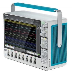 5 series mixed signal oscilloscope (MSO)
Tektronix’ 5 series MSO has a 396mm HD screen display with a capacitive pinch zoom-swipe touchscreen and front panel controls. Its 4, 6 or 8 FlexChannel inputs allow the measurement of one analogue signal or eight digital signals by just changing the probes. It has a 12-bit analogue-to-digital converter that delivers up to 16-bit of vertical resolution, making it easy for the user to check and measure even the minor details of the small signals that sometimes go unnoticed. Model numbers included in this series are MSO54, MSO56 and MSO58. They have an analogue bandwidth of about 350MHz to 2GHz and are capable of measuring record lengths of about 62.5 Mpoints to 125 Mpoints.
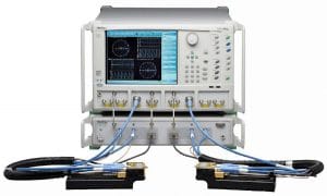 VectorStar broadband vector network analyser
Anritsu’s VectorStar is a vector network analyser (VNA) that has been upgraded recently to support the high data rate requirements of data centre cloud systems and 5G networks. This series has been introduced with universal fixture extraction (UFX) for engineers to evaluate designs more accurately and efficiently over extended periods of time. This helps the engineers to confidently set the product specifications, to test more products during production and to characterise the devices better. UFX adds additional advanced de-embedding tools to the series, thus improving the test fixture design, while the de-embedding of the test fixture improves the DUT (device under test) measurement accuracy. Company sources claim that this new VNA offers an opportunity to have high-speed data throughput products with competitive advantages, improves time to market just by improving first time yields, and offers improved model accuracy through improved test fixture de-embedding.
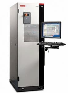 Keithley S540 parametric test system
Keithley S540 is a fully automated power semiconductor test system from Tektronix. Optimised to be used with the latest power semiconductor devices, the S540 allows high speed wafer level parametric testing of up to 48-pin semiconductors. This system works on semiconductor materials like gallium nitride (GaN) and silicon carbide (SiC). This wafer level testing enables profitable and optimised yields. It minimises the test set-up time, the test time and the floor space required, thus lowering the cost of ownership and achieving high voltage measurement performance. This test system also allows transistor capacitance measurements without any manual configuration of the test pins. The company claims that S540 can perform high voltage leakage current tests in less than 1 second.
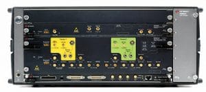 M8040A 64GBaud high performance PAM-4/NRZ BERT
The recently launched M8040A is an integrated BERT from Keysight for compliance testing and physical layer characterisation. It has been designed for test and R&D engineers for the characterisation of chips, transceiver modules, sub-components, boards, devices and systems with serial I/O ports. These I/O ports operate in the communications industry and at data centres with data rates up to 32GBaud and 64GBaud. The company claims that this device offers true error analysis along with accurate and repeatable results on optimising the performance margins of the 400GbE devices. It supports many popular standards that use data formats based on Pulse Amplitude Modulation-4 (PAM-4) and non-return-to-zero (NRZ), covering standards like 200GbE and 400GbE.
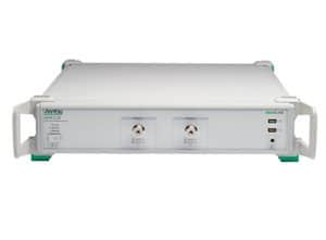 The MS46322B Shockline family of vector network analysers
Anritsu’s B series of Shockline vector network analysers has replaced the A series recently with completely new hardware and better specifications, compared to its legacy models. The company claims that the MS46322B series caters to applications in various fields and is suitable for testing cost-effective passive devices in engineering, manufacturing and education. This economical VNA has LRL (line-reflect-line), LRM (line-reflect-match) and SOLR (short-open-load-reciprocal) calibration capabilities, rather than the other calibration methods that need expensive and difficult-to-make waveguide loads. This series includes hardware enhancements that reduce the measurement speed from 220µs/point to 130µs/point. The MS46322B series is capable of addressing passive waveguide applications ranging from 8.5GHz to 43.5GHz in frequency.
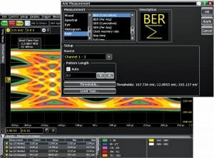 N8827A PAM-4 analysis software
N8827A is an analysis software for PAM-4 signals and is used in Infiniium real-time oscilloscopes. This software has been designed to quickly and accurately characterise the PAM-4 electrical signals described in IEEE 802.3bj Clause 94. PAM is a multi-level signalling format for increased bandwidth requirements in data centres to address the needs of future PAM measurements such as OIF-CEI-56G and IEEE 400G.
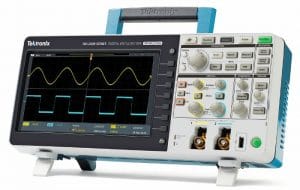 TBS2000 digital storage oscilloscope
TBS2000 from Tektronix is a digital storage oscilloscope with a recent upgrade on its firmware. This upgrade allows the oscilloscope to implement high resolution acquire mode, to support vertical fine scale, improve MPK knob usability and to support additional VPI probes. Its 228mm display with a 20 Mpoint record length allows it to capture more signals with high resolution. This oscilloscope allows accurate and easy design tests with features like on-waveform cursor readouts and 32 automated measurements. This device can be connected to a Wi-Fi network via a USB device and does not require any external power supply for its probes. This series covers four different models — TBS2072, TBS2102, TBS2074 and TBS2104, with a sample rate of up to 1GS/s.
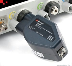 Keysight’s N7004A-33GHz optical-to-electrical converter
N7004A is a recently launched 33GHz optical-to-electrical converter from Keysight for its Infiniium real-time oscilloscope. This converter has a small form factor, and is used for characterisation and analysis of high-speed optical signals. The company claims that it is ideal for users to see the unfiltered response of optical transmissions. It has options for both single mode and multi-mode inputs.


