3D solder paste inspection systems have made the inspection process more accurate and precise, minimising the warping of the PCB.
By Sneha Ambastha
The miniaturisation of components and the complexity of circuit boards are increasing the importance of solder paste inspection. The main purpose of this inspection is to identify the volume and alignment of solder paste on the PCB. In order to make the connections between the surface mounted components and the PCB strong, it is very important that the right volume of solder paste is printed on the PCB. Printing a lower volume of solder paste may result in unreliable joints, while using too high a volume which is visible to the human eye, could leave the PCB stained. Special types of solder paste inspection systems, popularly called SPIs, are used for this type of work.
SPIs are mainly used with solder printing systems to improve the print quality and yield.
Over a period of time, SPIs have evolved from having only two dimensional (2D) capabilities to having three dimensional (3D) functions. The 3D version can measure the height/thickness of the solder paste printed on the PCB, which allows accurate detection of the volume of solder paste printed on it. 3D SPIs allow manufacturers to focus on following the lean assembly process, aiming for zero defects.
A few SPIs launched in the last one year
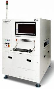
ViTrox’s V310i
V310i is an advanced, 3D solder paste inspection system from ViTrox launched in early 2016. Its D-lighting technology allows better image capture for data accuracy and error detection reports. Equipped with a fast Gerber switching system, V310i is considered to be an easy-to-use system that is convenient for editing. Company sources claim that the V310i is a system with high throughput and productivity for SMT production lines, because it uses powerful technologies.
 Key features
- Supports manual programming even without the Gerber database
- It’s D-lighting technology allows users a choice between three settings – black, normal and high brightness
- Can capture images from different light sources at different angles using CCD cameras
- Has an on-the-fly ‘bad mark detection’ feature to improve mounting efficiency
- Its one-button operation helps reduce training efforts dramatically
Key specifications:
Maximum board size: 510mm x 510mm with two projectors
Minimum board size: 50mm x 50mm
Maximum inspected area: 503mm x 510mm with two projectors
Maximum PCB warpage: ±5mm
Footprint (W x H x D): 1060mm x 1352mm x 2028mm
Weight: ~750kg
USP: Offers high throughput and productivity for SMT lines by using powerful technologies
Contact details: ViTrox Innovation Centre; Bayan Lepas, Malaysia; http://www.vitrox.com
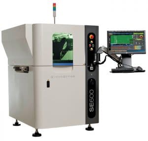
CyberOptics’ SE600
SE600 is a 3D SPI from CyberOptics, which was launched in June 2016 with new SPIV5 software. This software enables a fast and smart inspection process, and is supported by an intuitive interface for easy use and the shortest learning period. The machine allows its users to establish stencil cleaning cycles, optimise the printing process, and fine-tune the printer set-up procedure, apart from the other inspection work. The company claims that the SE600 is a single platform with exceptional usability and accuracy for niche markets like automotive, medical, military, etc.
 Key features
- Comes with a standard dual illuminated sensor designed for better reproducibility and repeatability, even on the smallest amount of paste deposited
- Its 3D sensing technology measures ‘true’ height with shadow-free imaging
- It is capable of offering full-fledged machine-level to factory-level statistical process control (SPC) with analysis and reporting tools
- Proactively analyses the accurate data trend and automatically optimises the printing process
- Its multi-touch software enables the shortest learning period for operators
Key specifications:
- Maximum panel size: 510mm x 510mm
- Minimum panel size: 50mm x 50mm
- Maximum inspection area: 508mm x 503mm
- Maximum PCB warpage:< 2 per cent of PCB diagonals or a maximum of 6.35mm
- Footprint: 1100mm x 1270mm x 1390mm
- Weight: ≈ 965kg
USP: Offers high speed inspection with accuracy and precision
Contact details: CyberOptics Corporation, Minnesota, United States; http://cyberoptics.com
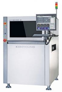
Koh Young’s KY8030-2
Improved in June 2016, KY8030-2 is a 3D SPI from Koh Young. Based on the dual projection technology, this system delivers accurate 3D inspection results without any shadow. It resolves shadow issues by utilising a two-way projection. It comes with a powerful printing process optimisation tool and supports the realisation of a smart factory with real-time process optimisation through SPC analytics.
 Key features
- Allows real-time measurement with PCB board warpage compensation using its multi-frequency technology
- Has intuitive software to support system usability and defect readability
- Uses 3D data and real images to detect a wide range of defects
- Supports process optimisation of pick-and-place machines, which control the panels that have defects
- Its KSMART link communication solution communicates with a wide range of production management systems
Key specifications:
Maximum PCB size:
- M: 330mm x 330mm
- L: 510mm x 510mm
- DL (Dual): 510mm x 320mm
- DL (Single): 510mm x 580mm
- XL: 850mm x 690mm
Minimum PCB size:
- M, L, DL: 50mm x 50mm
- XL: 70mm x 70mm
Maximum inspection size:
- Size: 10mm x 10mm
- Height: 400μm (2mm optional)
Footprint (W x D x H):
- M: 820mm x 1265mm x 1627mm
- L: 1000mm x 1265mm x 1627mm
- DL: 1000mm x 1445mm x 1627mm
- XL: 1350mm x 1445mm x 1627mm
Weight:
- M: 550kg L: 600kg DL: 700kg XL: 850kg
USP: 3D SPIs that offer accurate measurements and reliable inspection
Contact details: Koh Young Technology Inc., Seoul, Republic of Korea; http://www.kohyoung.com
India: NMTronics India Pvt Ltd, [email protected], www.nmtronics.com/smt/
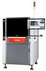
Parmi’s Sigma X Orange
Launched only a year ago in India, Sigma X Orange has got its software upgraded, which enables an improved camera scanning speed. The machine also has new hardware—a dual-lane option for a higher throughput with the same footprint. Sigma X Orange has been designed with electronic components that have been repositioned for easy access to the operating system. It shows 3D images of the defective pads by adjusting the viewing angle and the colour.
 Key features
- Has an inspection speed of about 10,000mm2/sec @ 10μm x 10μm, which is about 25 to 30 per cent faster than the RSC 6 sensor (available in its previous versions)
- It has an improved board transfer sequence that takes about 3-4 seconds less time than Parmi’s HS60 SPI
- Identifies total board warpage of up to 10mm (±5mm)
- Has an increased inspection area even though the dimensions of the machine have been reduced
- Provides accurate measurements, eliminating all the shadows with the help of its dual laser projection feature
Key specifications:
- Maximum PCB size: Standard: 480mm × 350mm (3-stage conveyor option: 350mm x 350mm)
Large: 580mm x 510mm - Minimum PCB size: 50mm x 50mm
Maximum PCB warpage: ±5mm (2 per cent) - Footprint (W x D x H): Standard: 850mm x 1205mm x 1510mm (3-stage conveyor option: 1210mm x 1205mm x 1510mm)
Large: 950mm x 1365mm x 1510mm - Weight:
Standard: 800kg Large: 900kg
USP: Delivers high accuracy and reliability with fast, stable and vibration-free motion
Contact details: Parmi Co. Ltd; Daejeon, Republic of Korea; http://www.parmi.com
India: Bergen Group India Pvt Ltd; [email protected]; http://www.bergengroupindia.com
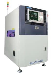
Aleader’s 5D SPI – ALD-ST3- 450
The 5D SPI -ALD-ST3-450 has been recently upgraded with new features and improvements. It has a completely new, modern, intuitive and transparent user interface for creating a new program in just few minutes. It has a real-time built-in SPC that allows constant monitoring of the printing process with the closed loop function. The company claims that any new user working on this will require a very short training period of just about an hour to learn how to program and use the system.
 Key features
- Comes with a unique algorithm for warpage compensation
- It has a simple user interface with the structured access level
- It has a real-time and easily readable SPC
- Programming on this is simple and takes less than 5 minutes
- Its bi-directional light projection eliminates shadow and irregular reflection effects
Key specifications:
Maximum PCB size: 50mm x 50mm
Minimum PCB size: 400mm x 450mm
(Max: 500mm – option)
Footprint (L x W x H):
1300mm x 900mm x 1527mm (excluding signal light tower height)
Weight: 790kg
USP: Transparent high resolution 2D image with stable and precise 3D measurement
Contact details: Aleader Europe Ltd; Europe; [email protected]; www.aleader-europe.com


